Research & Development
Creating customer value through technological innovation
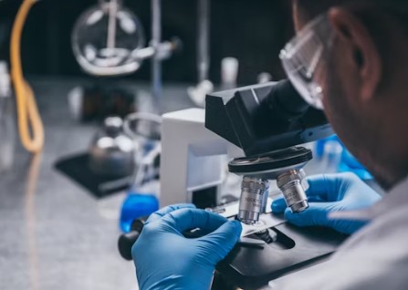
R&D Team
Experts leading next-generation semiconductor and display inspection technology
Optics R&D
Optical Design & Application
- Physics Major
- Optical Mechanism Design & Analysis
- Application Development
- Metrology Algorithm Development

SW R&D
Algorithm & O/S Application
- Mechatronics, Electronics Major
- IoT Device Development
- Deep Learning Algorithm
- 3D Inspection Algorithm Development

System R&D
System Design & Control HW
- Mechanical Engineering Major
- System Design & Analysis
- Precision Motion Analysis
- Development Algorithm Concept/Coding
Core Technology Capabilities
World-class technology based on Samsung Electronics equipment development experience
Wafer Inspection Technology
Accumulated development experience in semiconductor core process inspection equipment and process equipment technology such as Wafer defect inspector, wafer & photomask defect review SEM, dry etch (Applied to Samsung manufacturing lines, currently in mass production)
Precision Metrology Technology
Possessing high-precision, high-rigidity optical measurement system-based technology through the development of 8G Maskless lithography and UHV nm SEM equipment
In-situ Measuring Technology
Development and mass production of HBM Wafer Bonding in-situ measuring unit, OLED IGZO in-situ measuring unit technology